Simplify (using k-map) the given Boolean function in both SOP and POS using the don't care condition if: \(f(A, B, C, D) = ℼ(0,1,3,7,8,12) ℼ d(5,10,13,14)\).
Marks: 5Chapter: Unit 3: Combinational Logic Design
Comprehensive questions and detailed answers for Unit 3: Combinational Logic Design. Perfect for exam preparation and concept clarity.
Simplify (using k-map) the given Boolean function in both SOP and POS using the don't care condition if:
.
Define decoder. Draw logic diagram and truth table of 3 to 8 line decoder.
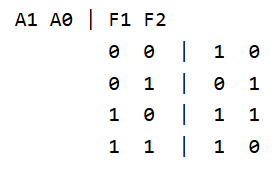
Define ROM. Implement the following combinational logic function using ROM:
Define PLA. Design PLA circuit with given function.
Design PLA Program table also.
Define universal gate. Explain Universal gates with their graphical symbol, algebraic expression, truth table, and Venn diagram.
Define Decoder. Explain binary to octal converter with block diagram, truth table and logic diagram.
Simplify the Boolean function F(w, x, y, z) = π(0,2,4,6,8,10,12,14) and don’t care conditions d(w, x, y, z) = π(1,3,9,11) using K-Map method for both SOP and POS form.
Define Multiplexer. Explain 4:1 multiplexer with its block diagram, truth table and logic diagram.
Simplify given Boolean function in both SOP and POS using k-map where d represents don't care condition.F (A, B, C, D) = ∏ (2, 3, 4, 5, 7, 9, 10) and ∏ d (0, 6, 11)
Define combinational logic circuit. Design a full adder with its truth table, logic diagram and Boolean expression.
Define Decoder. Design BCD to Decimal decoder with its block diagram, truth table, circuit diagram and mathematical expression.
Explain basic gates and universal gate. Realize NOR gate as a universal gate.
Explain PLA with its block diagram. Design a combinational circuit using a ROM that accepts a 3-bit number and generates an output binary number equal to the square of the input number with circuit diagram, truth table and block diagram.
Define multiplexer. Explain 4:1 multiplexer with its block diagram, truth table and logic diagram. Mention how a 4:1 multiplexer works like lower order multiplexer.
Simplify given Boolean function in both SOP and POS using k-map where d represents don't care condition.F (A, B, C, D) = ∏(0, 1, 3, 7, 8, 12) and ∏ d(5, 10, 13, 14)
Define combinational circuit. Write a combinational circuit design procedure. Design a half adder with its truth table, logic diagram and Boolean expression.
Define Priority encoder. Design 4:2 priority encoder with its block diagram, truth table, circuit diagram and mathematical expression.
Why NAND and NOR gates are called universal gates? Realize NAND gate as universal gate.
Define PLA with its block diagram. Realize BCD to gray code converter using PAL.
Explain the universal gates with their logic symbol, logic expression, and truth table. Realize an OR Gate using NAND Gate.
And more questions available on this page.